IVAM Microtechnology Network
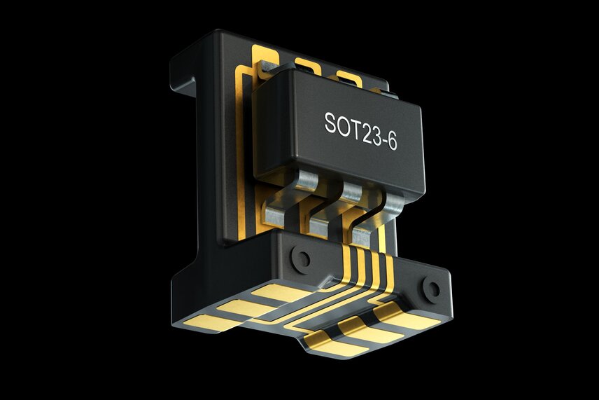
Flexible printed circuit boards made of thin polyimide films have established themselves in many product areas thanks to their application flexibility. Populating and assembling them, however, is decidedly more complex. This is where a new component carrier enters the picture.
By harnessing this all new HARTING development, electronic components can be fitted directly onto the component carrier, thereby replacing flexible circuit boards. The component carrier serves as a connecting element between the printed circuit board (PCB) and electronic components such as LEDs, ICs, photodiodes and sensors.The populated component carriers are delivered in tape & reel. In their standard design, the carriers can be processed in automatic assembly systems, just like other SMD electronic components. Two different sizes are currently available and can accommodate electronic components of standard size SOIC-8 and smaller. Moreover, HARTING can also produce the carriers in customer-specific sizes.
Three example applications where the component carrier can replace flexible circuit boards:
Thanks to the 3D-MID (mechatronic integrated device) technology, electronic components can be fitted directly onto a three-dimensional body without the need for circuit boards or connecting cables. The base body is produced through injection molding, whereby the thermoplastic is provided with a non-conductive, inorganic additive. In order for this material to be able to accommodate electrical circuits, the additives in the plastic are “activated” through laser direct structuring (LDS). In this process, the laser beam writes the areas intended for the conductive tracks and creates a micro-rough structure. The metal particles released in the process form the nuclei for the subsequent chemical metallization. This process creates electrical traces across the three-dimensional base body. The plastic employed offers high thermal stability and can therefore be soldered in the reflow oven.
The component carrier developed by this process is suitable for various applications. It can be equipped with several sensors that, if desired, could be aligned in three directions to take measurements in three axes (X, Y, Z). Components can be fitted simultaneously on two parallel surfaces on the front and back sides, as well as on the end face. HARTING has submitted a patent application for the component carrier.
In an automated process, HARTING fits electronic components such as LEDs, ICs, photodiodes and sensors directly on the component carrier. The total cost of the component carrier is two-thirds lower than those of flexible PCB solutions. This is due to the fact that it eliminates the frequently complex handling involved with flexible printed circuit boards, e.g. populating, gluing and assembling. The process even delivers benefits in small volumes, as the component carrier can be used for different applications without adaptation, thereby eliminating the costs of a new injection mold. Compared with flexible printed circuit boards, this process achieves more precise component positioning, greater repeatability and better quality.
Contact: Thomas Hess, HARTING AG Biel
Thomas.Hess@HARTING.com

Change in the institute management: The Executive Board of the Fraunhofer-Gesellschaft has appointed Prof. Holger Kapels as managing director of …
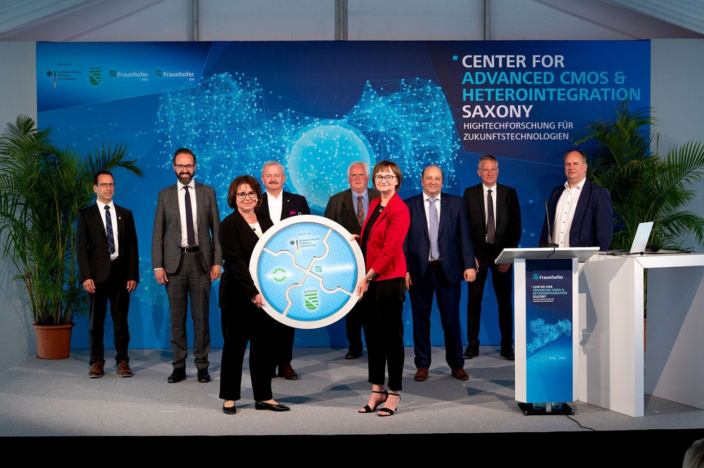
A flagship of semiconductor research with international reach is emerging in Dresden. Fraunhofer IPMS and Fraunhofer IZM-ASSID are bundling their …
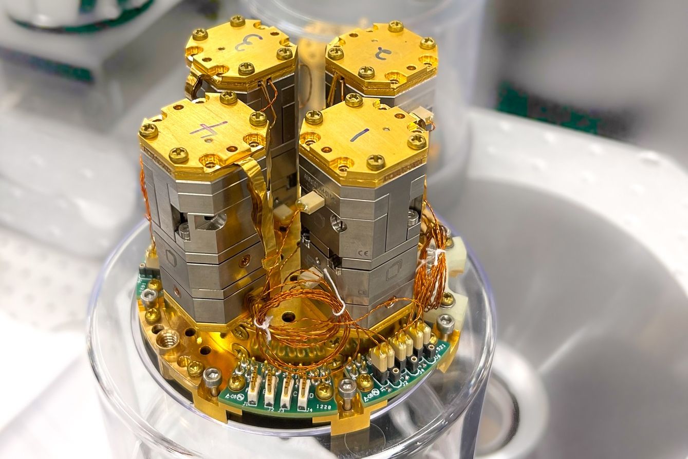
The demand for electronics that operate at low temperatures is growing and becoming ever more important, especially for applications in …